
Introducing the NVIDIA GeForce RTX 4080 Series
▲ GeForce RTX 40 series (4080 / 4090)
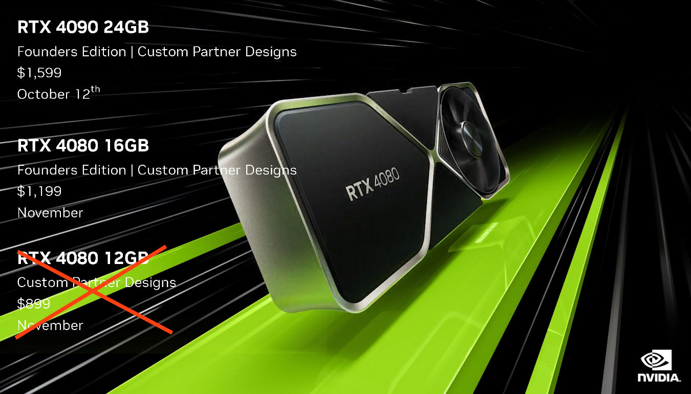
Immediately after the launch of the GeForce RTX 4090 in October, NVIDIA released the GeForce RTX 4080 series on the 15th, using the new Nvidia Ada Lovelace GPU micro-architecture. There were originally two models in this series, the RTX 4080 16GB with the AD103 graphics core and the AD104 graphics core. RTX 4080 12GB, the graphics core, is also called RTX 4080, but the specifications and performance of the two are quite different. Many netizens accused the models of confusion. In the end, NVIDIA officially canceled the launch plan of RTX 4080 12GB, and only retained the GeForce RTX 4080 16GB model.
Compared to the previous Ampere GPU architecture, NVIDIA Ada Lovelace GPUs are up to 2X faster in rasterized games and up to 4X faster in ray-traced games, representing the largest generational performance upgrade in NVIDIA history (each generation It’s all said like this XD), mainly four key innovations:
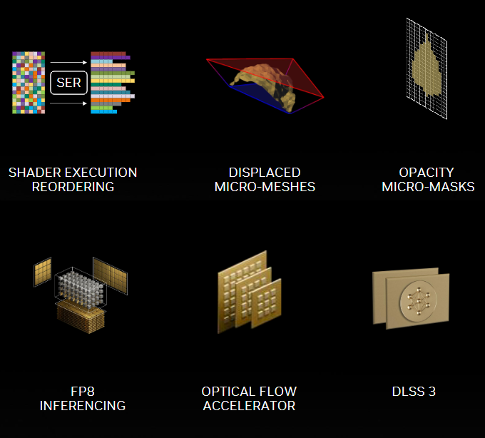
Revolutionary Architecture Scale Up:
The scale of the Ada Lovelace GPU architecture has been greatly improved. Under the process innovation, NVIDIA engineers can manufacture 76.3 billion transistors, up to 18,432 CUDA Core chips, and can run more than 2.5GHz clock pulse, but can maintain the same level as GeForce RTX 3090 Ti The same 450W TGP power consumption performance.
More powerful Ada Lovelace RT Core :
In order to achieve more powerful ray tracing capabilities, the Ada Lovelace GPU architecture upgrade 3rd generation RT Core has added two new hardware units; Opacity Micromap Engine can increase the ray tracing speed of alpha-tested geometry by 2 times, and Displaced Micro- Mesh Engine can generate Displaced Micro-Triangles in real time to create additional geometry, which can greatly increase the complexity of ray tracing without burdening GPU performance and storage.
The shader performs the reordering:
The SM of the Ada Lovelace GPU architecture supports shader execution reordering, which can dynamically organize and reschedule the workload of the shader, greatly improving the shading efficiency of ray tracing. In Cyberpunk’s RT:Overdrive mode, the performance is improved compared with the previous generation SM 44%.
NVIDIA DLSS 3 technology:
The Ada Lovelace GPU architecture adds DLSS 3 technology, upgrades the 4th generation Tensor Cores, and adds a new optical flow accelerator that can provide AI frame generation, which can increase the frame rate of DLSS 3 to twice that of the previous DLSS 2.0 while maintaining Or exceed native image quality, and add FP8 tensor computing capability, compared with traditional brute-force graphics rendering, DLSS 3 ultimately speeds up by 4 times, while providing low system latency.
▲ GeForce RTX 4080 series officially debut
NVIDIA officially released the GeForce RTX 4080 model on the 16th, based on the AD103 graphics core, with 9,728 CUDA Cores, 16GB GDDR6X capacity, MSRP priced at US$1,199, the performance is twice that of the previous generation RTX 3080 Ti, but the GP power consumption is reduced by 10%. If the game performance is started at 4K + RT, it can reach 1.5 times that of RTX 3080 Ti.
It was originally planned to release the GeForce RTX 4080 12GB model on the same day, but due to fierce opposition from the outside world, NVIDIA finally decided to cancel the GeForce RTX 4080 12GB, and it is very likely that it will be listed under the name of GeForce RTX 4070 Ti in January next year, but the specifications will not change. Undecided.
TSMC 4N process, NVIDIA AD103 graphics core
NVIDIA AD103 graphics core is based on the new Ada Lovelace micro-architecture and is used in GeForce RTX 4080 products. The performance improvement mainly comes from the number of FP32 computing units and the multiplication of clocks, larger L2 Cache capacity and new shader execution sorting technology. 3rd generation RT Cores, upgraded 4th generation Tensor Cores, compared with the previous generation Ampere GPU micro-architecture, the traditional raster graphics operation has been improved by 2 times, and the ray tracing performance has been improved by nearly 4 times.
GeForce RTX 4080 uses AD103-300 graphics core, adopts TSMC 4N NVIDIA Custom process, has 45.9 billion transistors, Die Size 379mm² Compared with the GA102-200 Die Size 628mm² of the previous generation GeForce RTX 3090, it is much smaller, and a complete AD103 chip is built-in 7 GPC units, 42 TPC texture processing clusters and 84 SM stream multiprocessors, with 10752 CUDA Cores, 84 RT Cores and 336 Tensor Cores.
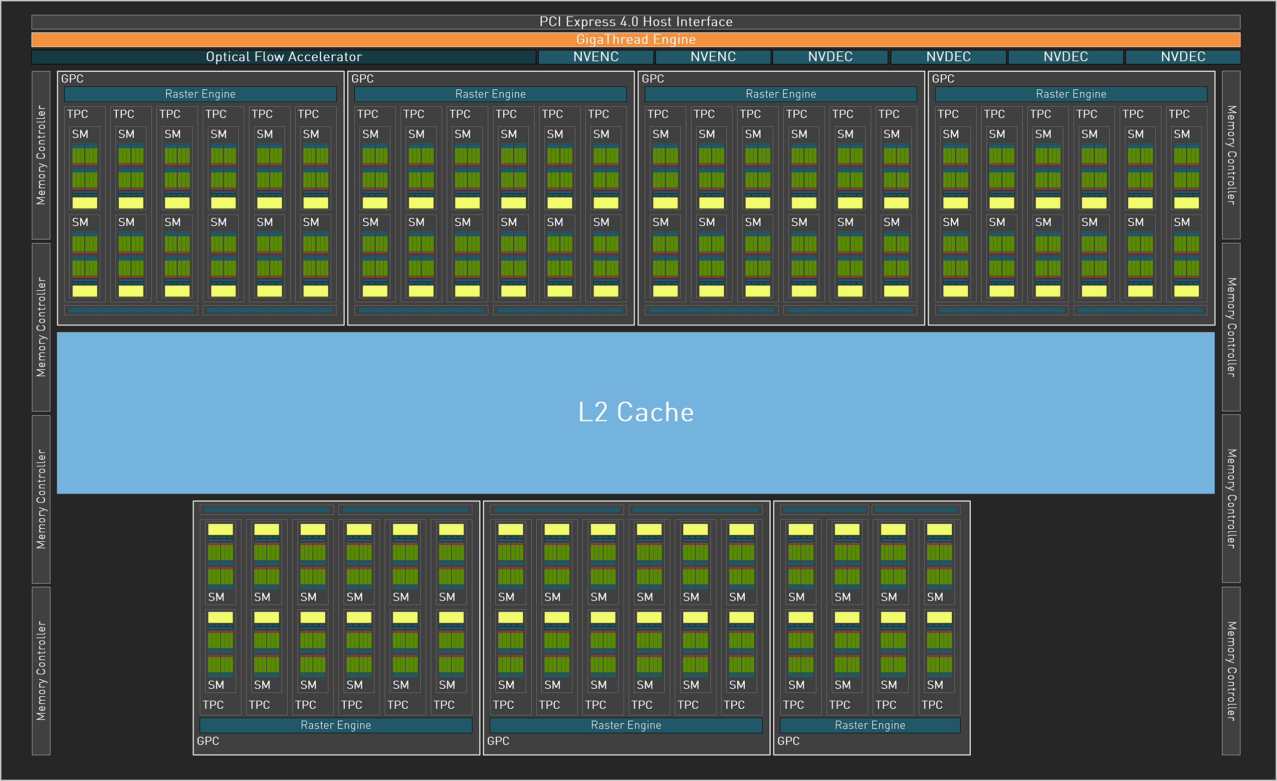
▲ NVIDIA AD103 Block Diagram
However, some units of GeForce RTX 4080 have been shielded. Although 7 GPC units are maintained, it is reduced to 38 TPC texture processing clusters and 76 SM stream multiprocessors, with 9,278 CUDA Cores, 76 RT Cores and 304 Tensor Cores.
In terms of core clock, the use of TSMC 4N process makes the core clock of this generation of Ada Lovelace can be greatly increased. The default clock of GeForce RTX 4090 is 2,205MHz, the boost clock is 2,505MHz, and the highest TDP is 320W.
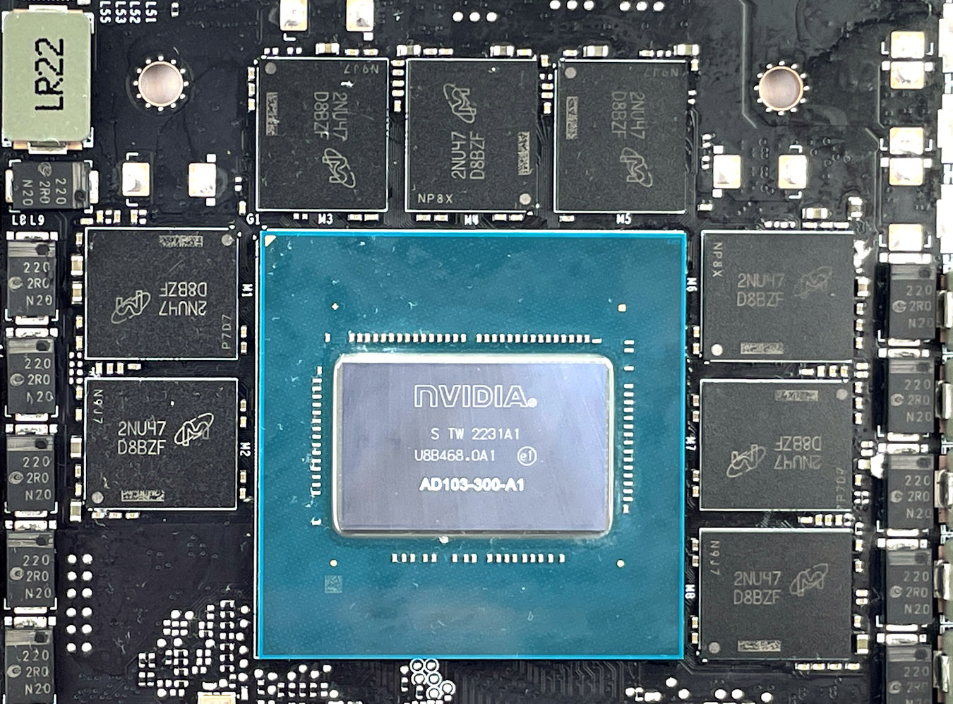
▲ NVIDIA AD103-300-KA-A1 graphics core
In terms of memory, GeForce RTX 4080 uses higher-speed 22.4Gbps GDDR6X memory particles. Although the memory capacity is increased to 16GB, the memory bandwidth is reduced to 256bit, and the total memory bandwidth is reduced to 716.8GB/s. It is less than the 760GB/s of the RTX 3080, but one of the major improvements of Ada Lovelace is the substantial increase in the L2 Cache capacity. The L2 Cache of the previous generation RTX 3080 was only 5120KB, and the current generation RTX 4080 has greatly increased to 65536 KB. Compared with AMD’s Infinity As an L3 Cache, Cache has higher efficiency, which can greatly increase the game workload data hit rate, reduce read latency and reduce GDDR6X memory bandwidth usage.
NVIDIA GeForce RTX 40 Family Full Specifications
| GPU Codename | AD104 | AD103 | AD102 |
| GPU Architecture | NVIDIA AdaLovelace |
NVIDIA There’s Lovelace |
NVIDIA There’s Lovelace |
| GPCs | 5 | 7 | 11 |
| TPCs | 30 | 38 | 64 |
| SMs | 60 | 76 | 128 |
| CUDA Cores / SM | 128 | 128 | 128 |
| CUDA Cores / GPU | 7680 | 9728 | 16384 |
| Tensor Cores / SM | 4 (4th Gen) | 4 (4th Gen) | 4 (4th Gen) |
| Tensor Cores / GPU | 240 (4th Gen) | 304 (4th Gen) | 512 (4th Gen) |
| RT Cores | 60 (3rd Gen) | 76 (3rd Gen) | 128 (3rd Gen) |
| GPU Boost Clock (MHz) | 2610 | 2505 | 2520 |
| Peak FP32 TFLOPS (non-Tensor) | 40.1 | 48.7 | 82.6 |
| Peak FP16 TFLOPS (non-Tensor) | 40.1 | 48.7 | 82.6 |
| Peak BF16 TFLOPS (non-Tensor) | 40.1 | 48.7 | 82.6 |
| Peak INT32 TOPS (non-Tensor) | 10.6 | 24.4 | 41.3 |
| RT TFLOPS | 92.7 | 112.7 | 191 |
| Peak FP8 Tensor TFLOPS with FP16 Accumulate |
320.7/641.4 | 389.9/779.8 | 660.6/1321.2 |
| Peak FP8 Tensor TFLOPS with FP32 Accumulate |
320.7/641.4 | 389.9/779.8 | 660.6/1321.2 |
| Peak FP16 Tensor TFLOPS with FP16 Accumulate |
160.4/320.8 | 194.9/389.8 | 330.3/660.6 |
| Peak FP16 Tensor TFLOPS with FP32 Accumulate | 80.2/160.4 | 97.5/195 | 165.2/330.4 |
| Peak BF16 Tensor TFLOPS with FP32 Accumulate |
80.2/160.4 | 97.5/195 | 165.2/330.4 |
| Peak TF32 Tensor TFLOPS | 40.1/80.2 | 48.7/97.4 | 82.6/165.2 |
| Peak INT8 Tensor TOPS | 320.7/641.4 | 389.9/779.82 | 660.6/1321.2 |
| Peak INT4 Tensor TOPS | 641.4/1282.8 | 779.8/1559.6 | 1321.2/2642.4 |
| Frame Buffer Memory Size and Type | 12GB GDDR6X | 16GB GDDR6X | 24GB GDDR6X |
| Memory Interface | 192-bit | 256-bit | 384-bit |
| Memory Clock (Data Rate) | 21 Gbps | 22.4 Gbps | 21 Gbps |
| Memory Bandwidth | 504 GB/sec | 716.8 GB/sec | 1008 GB/sec |
| ROPs | 80 | 112 | 176 |
| Pixel Fill-rate (Gigapixels/sec) | 208.8 | 280.6 | 443.5 |
| Texture Units | 240 | 304 | 512 |
| Texel Fill-rate (Gigatexels/sec) | 626.4 | 761.5 | 1290.2 |
| L1 Data Cache/SharedMemory | 7680 KB | 9728 KB | 16384 KB |
| L2 Cache | 49152 KB | 65536 KB | 73728 KB |
| Register File Size | 15360 KB | [19456KB | 32768 KB |
| Video Engines | 2x NVENC (Gen 8) 1x NVDEC (Gen 5) |
2x NVENC (Gen 8) 1x NVDEC (Gen 5) |
2x NVENC (Gen 8) 1X NVDEC (Gen 5) |
| TGP Power | 285W | 320W | 450W |
| Transistor Count | 35.8 Billion | 45.9 Billion | 76.3 Billion |
| Die Size | 294.5mm² | 378.6mm² | 608.5mm² |
| Manufacturing Process | TSMC 4N | TSMC 4N | TSMC 4N |
| PCIe Interface | Gen4 | Gen4 | Gen 4 |