
Introducing the NVIDIA GeForce RTX 4070 Series
NVIDIA officially released the performance-level GeForce RTX 4070 graphics card on the 13th. It adopts AD104-250 graphics core, has 5,888 CUDA Cores, 192bit interface and 12GB GDDR6X memory capacity. It is priced at US$599 and will replace GeForce RTX 3070 Ti. In the game market, with the light-tracking special effects fully enabled, 100fps+ performance can be achieved through the blessing of DLSS3 technology. More importantly, the power consumption of the entire card is reduced to 200W TGP, which is as high as 290W TGP compared with the previous generation RTX 3070 Ti, and the performance-to-power ratio has been further improved.
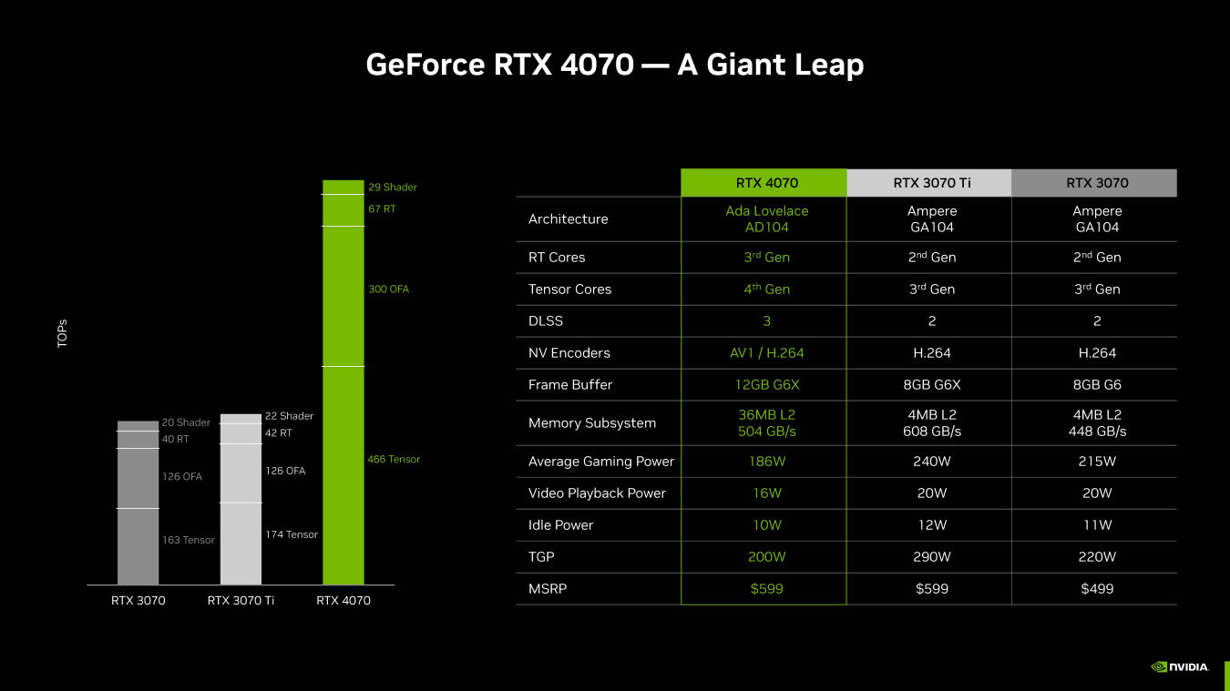
Analyzing the design direction of NVIDIA GeForce RTX 4070 chip, although the performance of Shader operation (29 TOPS) and RT operation (67 TOPS) has improved compared with RTX 3070 Ti, the more obvious progress lies in Tensor matrix operation (466 TOPS) and OFA optical flow In terms of accelerated computing (300 TOPS), the game performance increase after DLSS is activated is more obvious, and it also provides stronger AI computing capabilities.
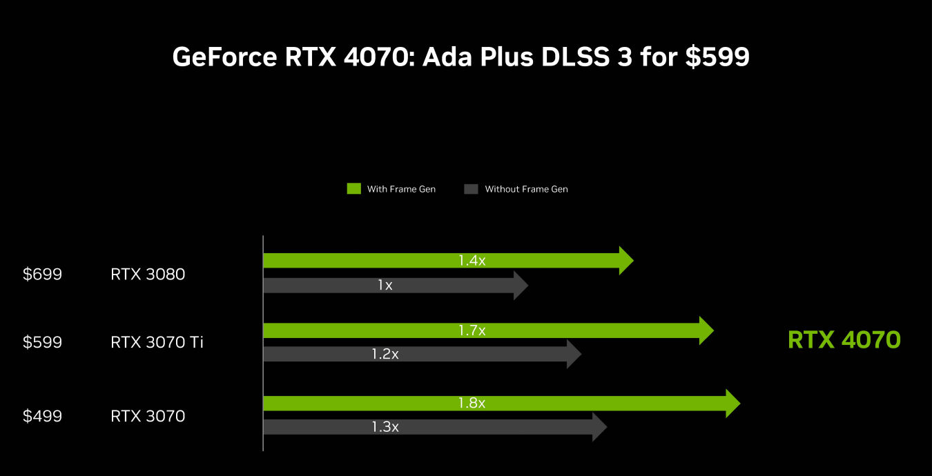
That’s right, the performance improvement of GeForce RTX 4070 is very focused on DLSS 3 technology. What if there is no DLSS 3 blessing? According to NVIDIA’s official data, when the Frame Gen of DLSS 3 is enabled, GeForce RTX 4070 is faster than GeForce RTX 3080 on average at 2K resolution 40%, without DLSS 3, it can only be tied with GeForce RTX 3080. Therefore, the success of GeForce RTX 4070 in the game market depends largely on the popularity of NVIDIA DLSS 3 technology.
TSMC 4N process, NVIDIA AD104-250 graphics core
The NVIDIA AD104 graphics core is based on the new Ada Lovelace micro-architecture and is used in GeForce RTX 4070 and RTX 4070 Ti products. The performance improvement mainly comes from the number of FP32 computing units and the multiplication of clocks, larger L2 Cache capacity and new shader execution sequencing technology. Technology, upgrade the 3rd generation RT Cores, upgrade the 4th generation Tensor Cores, compared with the previous generation Ampere GPU micro-architecture, the traditional raster graphics operation has been improved by 2 times, and the ray tracing performance has been improved by nearly 4 times.
Using TSMC 4N NVIDIA Custom process, with 35.8 billion transistors, Die Size 294.5mm² similar to the GA106-300 Die Size 276mm² of the previous generation GeForce RTX 3060, the complete AD104 chip built-in 5 GPC units, 30 TPC texture processing clusters and 60 SM stream multiprocessors with 7,680 CUDA Cores, 60 RT Cores and 240 Tensor Cores.
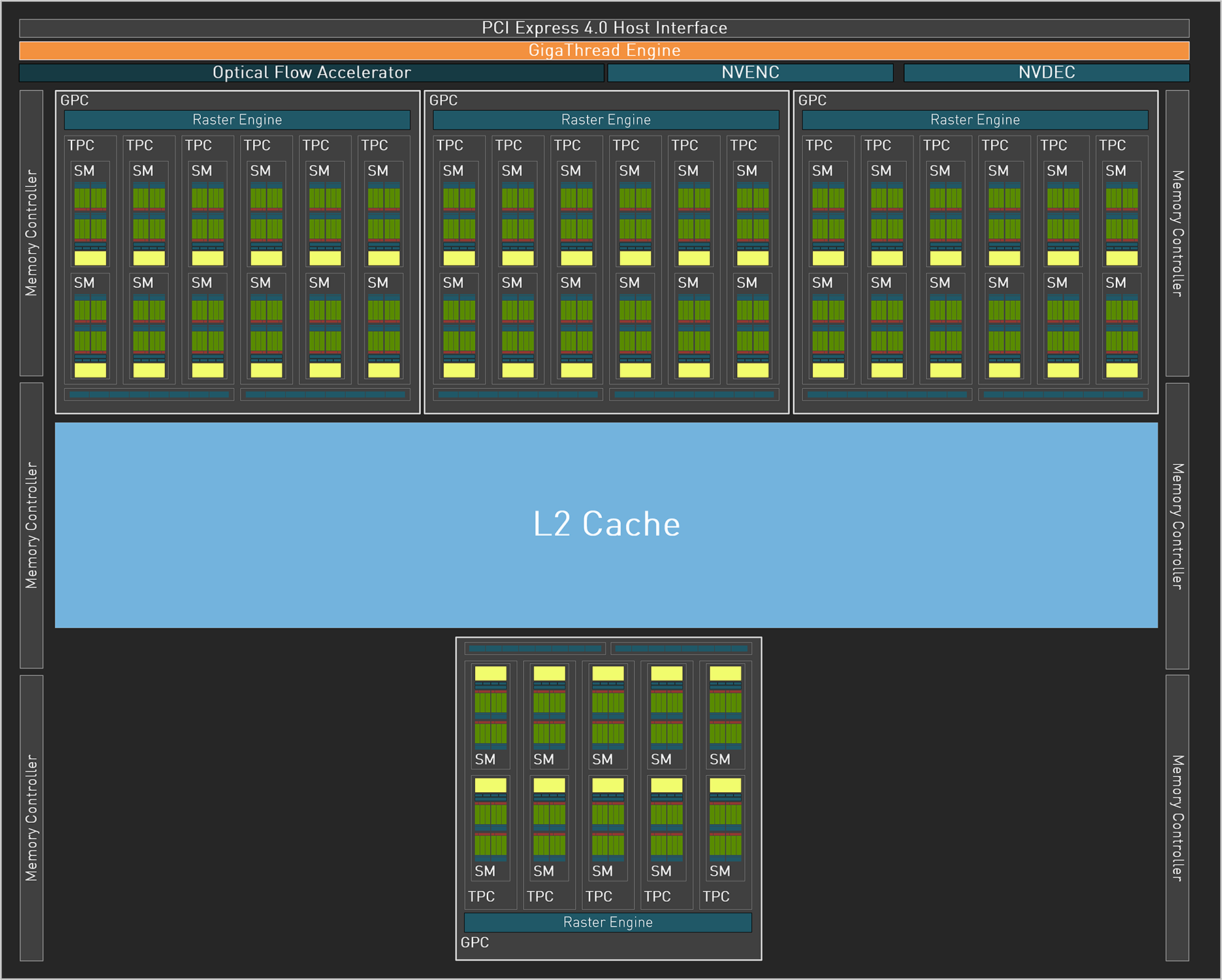
▲ NVIDIA AD104-250 Block Diagram
GeForce RTX 4070 uses the AD104-250 graphics core to make cuts, down to 4 GPC units, but reduced to 23 TPC texture processing clusters and 46 SM stream multiprocessors, with 5,888 CUDA Cores, 46 RT Cores , 184 Tensor Cores, 184 Texture Units and 64 ROPs.
In terms of core clock, the use of TSMC 4N process makes the core clock of this generation of Ada Lovelace can be greatly increased. NVIDIA GeForce RTX 4070 FE has a default clock of 1,920MHz, a boost clock of 2,475MHz, and a maximum TDP of 200W.
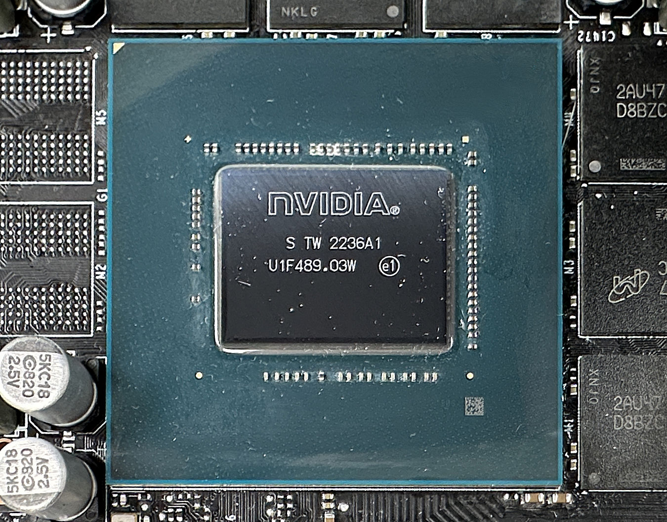
▲ NVIDIA AD104 graphics core
In terms of memory, NVIDIA GeForce RTX 4070 maintains the same 192-bit memory interface as RTX 4070 Ti, with 21Gbps GDDR6X memory particles, and the highest memory bandwidth is 504GB/s, although the previous generation GeForce RTX 3070 uses 256-bit memory , but using slower 14Gbps GDDR6 memory particles, the memory bandwidth is only 448GB/s, which is lower than GeForce RTX 4070.
In addition, one of da Lovelace’s major improvements is the substantial increase in L2 Cache capacity. The L2 Cache of the previous generation RTX 3070 was only 4096 KB, while the current generation RTX 4070 has been greatly increased to 36864 KB, which is more efficient than AMD’s Infinity Cache as L3 Cache. It can greatly increase the hit rate of game Workload data, reduce the reading delay and reduce the bandwidth usage of GDDR6X memory.
NVIDIA GeForce RTX 40 Family Full Specifications
| GPU Codename | AD104 | AD104 | AD103 | AD102 |
| GPU Architecture | NVIDIA There’s Lovelace |
NVIDIA There’s Lovelace |
NVIDIA There’s Lovelace |
NVIDIA There’s Lovelace |
| GPCs | 4 | 5 | 7 | 11 |
| TPCs | 23 | 30 | 38 | 64 |
| SMs | 46 | 60 | 76 | 128 |
| CUDA Cores / SM | 128 | 128 | 128 | 128 |
| CUDA Cores / GPU | 5888 | 7680 | 9728 | 16384 |
| Tensor Cores / SM | 4 (4th Gen) | 4 (4th Gen) | 4 (4th Gen) | 4 (4th Gen) |
| Tensor Cores / GPU | 184 (4th Gen) | 240 (4th Gen) | 304 (4th Gen) | 512 (4th Gen) |
| RT Cores | 46 (3rd Gen) | 60 (3rd Gen) | 76 (3rd Gen) | 128 (3rd Gen) |
| Frame Buffer Memory Size and Type | 12GB GDDR6X | 12GB GDDR6X | 16GB GDDR6X | 24GB GDDR6X |
| Memory Interface | 192-bit | 192-bit | 256-bit | 384-bit |
| Memory Clock (Data Rate) | 21 Gbps | 21 Gbps | 22.4 Gbps | 21 Gbps |
| Memory Bandwidth | 504 GB/sec | 504 GB/sec | 716.8 GB/sec | 1008 GB/sec |
| ROPs | 64 | 80 | 112 | 176 |
| L1 Data Cache/SharedMemory | 5888 KB | 7680 KB | 9728 KB | 16384 KB |
| L2 Cache | 36864 KB | 49152 KB | 65536 KB | 73728 KB |
| Register File Size | 11776 KB | 15360 KB | [19456KB | 32768 KB |
| Video Engines | 2x NVENC (Gen 8) 1x NVDEC (Gen 5) |
2x NVENC (Gen 8) 1x NVDEC (Gen 5) |
2x NVENC (Gen 8) 1x NVDEC (Gen 5) |
2x NVENC (Gen 8) 1X NVDEC (Gen 5) |
| TGP Power | 200W | 285W | 320W | 450W |
| Transistor Count | 35.8 Billion | 35.8 Billion | 45.9 Billion | 76.3 Billion |
| Die Size | 294.5mm² | 294.5mm² | 378.6mm² | 608.5mm² |
| Manufacturing Process | TSMC 4N | TSMC 4N | TSMC 4N | TSMC 4N |
| PCIe Interface | Gen4 | Gen4 | Gen4 | Gen4 |